During wafer processing, defective products due to the influence of pollutants account for more than 50% of the production loss. The production process of wafer begins with silicon rods being ground, polished, sliced and coated to form silicon wafers. The silicon wafer is then photoresist, photoresist, ion injection, electroplating, polishing and slicing to form a single wafer. Each of these steps has the potential to produce deadly pollution.

The common surface pollution of wafer is divided into metal pollution, organic pollution and particle pollution. Among them, metal pollution can lead to leakage current, because metal combined with air to form oxides will reduce the voltage, resulting in a reduced cycle cycle of current-carrying electrons. The pollution of organic matter will reduce the hydrophilicity of wafer surface, forming a hydrophobic layer adhering to the surface, increasing the roughness and destroying the growth structure of epitaxial layer. In addition, the presence of organic pollutants will also affect the cleaning effect of metal pollutants resulting in superimposed pollution. Particle pollution can lead to blocking or obscuration in the etching process and pinholes and microholes in the deposition process. If the particle diameter is large or has electrical conductivity, it will also lead to short circuit.

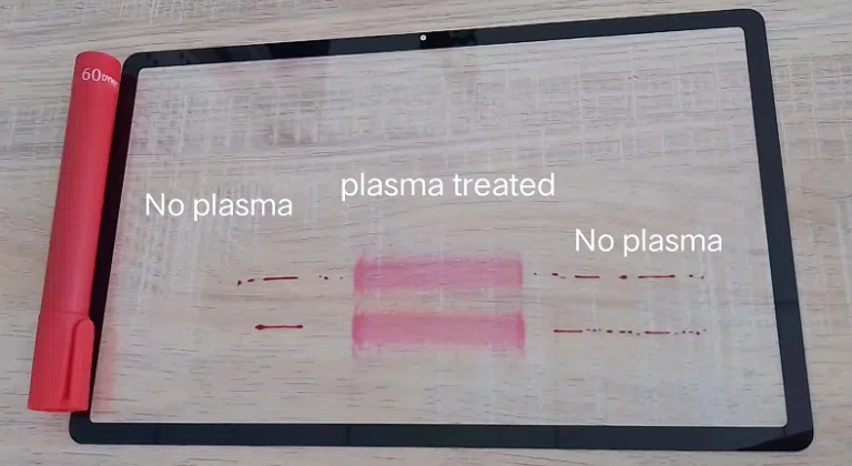
Therefore, the cleaning of pollutants is a problem that must be faced. Wafer surface cleaning can be divided into wet cleaning and dry cleaning, while dry cleaning plasma cleaning has higher removal efficiency for organic pollutants. The organic pollutants on wafer surface include grease, photoresist, cleaning solvent, etc. Especially for the removal of photoresist, plasma cleaning technology has a good effect. This is because the photoresist can be quickly volatilized into gaseous substances under the action of strong oxygen ions, so as to achieve the effect of removal. For the removal of particles and metal pollutants, plasma cleaning machine can be used for partial cleaning through physical and chemical action, but for complete cleaning, plasma can be used to improve the hydrophilicity of the wafer surface and promote the cleaning of the wafer with hydrogen peroxide, so that the surface can be thoroughly cleaned.
With the chip getting smaller and smaller, the drying technology of wet process is facing more and more challenges, and the advantages of dry cleaning are becoming more and more prominent. Its advantages of convenient operation, high efficiency, safety, no pollution, stable quality and so on, plasma treatment for wafer is more and more used in the semiconductor industry.
Using GD-10 RF plasma cleaner machine to removel the photoresist is very suitable. If you have interested about it, feel free to contact me.