Skip to content
  • Home
  • Product
    • Atmospheric Plasma
    • Vacuum Plasma Cleaner
    • Equipment Matching Customization
  • Application
    • Printing & Packing Industry
    • Textiles Industry
    • Semiconductor Industry
    • Plastic & Rubber Industry
    • Optics Industry
    • New Energy Industry
    • Home Appliances Industry
    • Wire & Cable Industry
    • Biomedical Industry
    • Automotive Industry
  • Case Study
  • Resource
    • Blog
    • Technical Training
  • About
  • Contact
Send Inquiry

Home  ❯  Case Study  ❯  GD -30 Vacuum Plasma Cleaner for PCB to Remove the Residue

GD -30 Vacuum Plasma Cleaner for PCB to Remove the Residue

plasma cleaner for PCB cleaning
Project Summary
  • Technology: Plasma etching and cleaning
  • Treatment Material: PCB
  • Treatment Purpose: remove residue and than electroplate
  • Device Model: GD-30 plasma cleaner

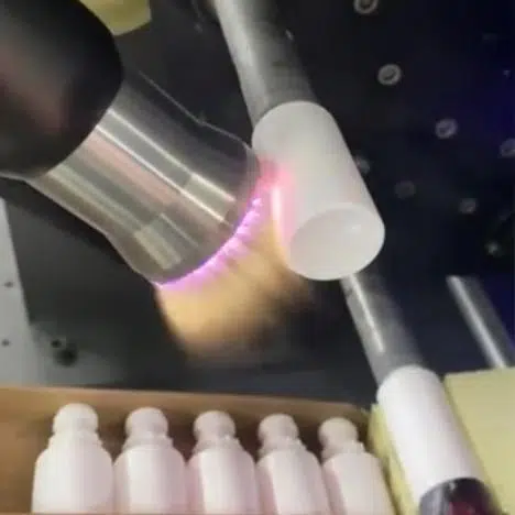
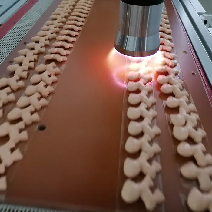
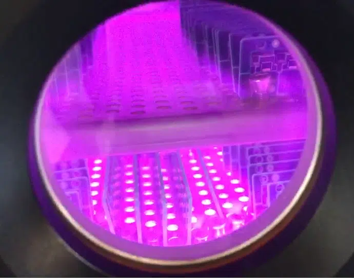
GD-30 Plasma Cleaning Machine is consist of the plasma cleaner host and a vacuum pump. The vacuum cavity size is 350(L)*320(W)*320(H) mm, and the equipment size is 870(L)*740(W)*1540(H) mm. What’s more, we can customized the layer, cavity size and the power frequency with customers. With PLC and touch screen control, it’s very convenient.

plasma cleaning machine

It can be used for large-scale continuous production and various of products.

PCB, called printed circuit board, is the carrier of electronic components and electrical appliances connected with each other. There are three categories: single panel, double panel and multi-layer board. The production process of multi-layer PCB is very complex, mainly including PCB layout, core plate making, core plate drilling and inspection, lamination, drilling, copper chemical precipitation of the hole wall, outer PCB etching and other processes. The main function of the plasma cleaning machine is to remove the residual glue of the hole wall and improve the activity in the hole after drilling, so that the liquid can fully clean the hole wall and improve the conductive performance of PCB.

plasma for PCB

In fact, the multilayer plate is made of copper clad plate (core plate), copper foil and semi-solidified plate . Taking 4 layers of PCB as an example, it is made of 1 piece of copper clad plate and 2 pieces of copper foil, and then bonded with semi-solidified plate. Semi-cured sheet is generally epoxy resin material with insulation, under the action of pressure can make the core plate and copper foil fixed. In order to connect different layers of lines will be drilled on the PCB, and then electroplating in the hole wall, so that the hole wall can be conductive. Residual glue is the epoxy resin glue remaining on the hole wall after drilling. The epoxy resin glue is an insulating impurity.

If it is not removed thoroughly, it will lead to the following four problems.

  1. Combined with other agents produce greater pollution
  2. The corrosion of lines and devices, damage the electrical performance of components
  3. Impact the effect of plating and chemical copper, cause quality hidden trouble
  4. Bond between copper foil and copper plate is not strong, make liquid deep, affect the subsequent etching.

plasma cleaner for PCB cleaning

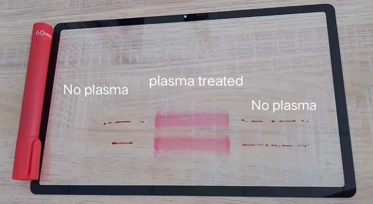
Plasma cleaner can remove part of the epoxy resin glue, but can not be thoroughly cleaned, so it must use potassium permanganate and other acid for thoroughly remove. Due to the active function of the plasma, the activity of the pore wall surface is changed and improving the hydrophilic nature of the surface, so that the liquid liquid can be cleaned more thoroughly. Plasma cleaning is divided into three aspects, activation, removal and decontamination. First, the plasma produced by nitrogen electrolysis makes the PCB surface in an active state; Second, the plasma produced by mixing oxygen and CF4 reacts with the adhesive residue and glass fiber; Three, when oxygen is the main gas, the oxygen ion and the residue on the material surface to achieve the cleaning effect.

Noted: We have obtained the customer’s consent before sharing this item. We never sell any customer information. If you want to share this project, please get our consent first.

  • Get A Quote

Related Case

Plasma Treatment Is Necessary For Surface Activation

How to Test the Effect after the Plasma Treatment

  • Technology: Plasma activate and modified
  • Treatment Material: Plastic, Metal, Chips, PCB, Glass
  • Treatment Purpose: Improve the Hydrophilic
  • Device Model: Plasma Treatment Machine
plasma for PDMS bonding

The Key Role of FARI Plasma Cleaning Machine in PDMS Bonding

  • Technology: Plasma activate and modified
  • Treatment Material: PDMS
  • Treatment Purpose: PDMS Binding
  • Device Model: GD-5 Vacuum Plasma Cleaner

PM-G13A Low Temperature Plasma Treatment PP Cosmetic for Improve Screen Printing Adhesion

  • Technology: Plasma activate and modified
  • Treatment Material: PP
  • Treatment Purpose: Improve printing adhesion
  • Device Model: PM-G13A Atmospheric plasma treatment machine
atmospheric plasma treatment for ABS

How the Effect of ABS can be Reach 60 Dyne After Treated by Atmospheric Plasma

  • Technology: Plasma activate and modified
  • Treatment Material: ABS
  • Treatment Purpose: Improve printing adhesion
  • Device Model: PM-G13A Atmospheric plasma treatment machine
plasma surface treatment for LED

Plasma Surface Treatment for LED Lamp Strip

  • Technology: Plasma activate and modified
  • Treatment Material: silicone rubber
  • Treatment Purpose: Improve bonding strength
  • Device Model: PM-G13A Atmospheric plasma surface treatment machine
plasma for wafer to removel the photoresist

Plasma Treatment for Wafer Cleaning in the Semiconductor Industry

  • Technology: Plasma etching, activation and cleaning
  • Treatment Material: Wafer
  • Treatment Purpose: Improve the Hydrophilic
  • Device Model: GD-10 RF Vacuum Plasma Cleaning machine
plasma treat for wire and cable

How to Solve the Problem of Inkjet Code Come Off from the Wire & Cable

  • Technology: Plasma surface activate
  • Treatment Material: PVC, PE, PA
  • Treatment Purpose: Improve adhesion of inkjet code
  • Device Model: Atmospheric plasma surface treatment machine of GM-2000
plasma for sound basin

How to improve the bonding strength of rubber sound basin?

  • Technology: Plasma cleaning
  • Treatment Material: Rubber
  • Treatment Purpose: Improve bonding strength
  • Device Model: GD-10 Vacuum Plasma Cleaning machine

Fari was founded in 2011, is a professional manufacturing enterprise specializing in the research and development, production, sales and promotion of vacuum plasma cleaner and atmospheric plasma surface treatment technology equipment. 

  • sales@szfangru.com
Linkedin Youtube
Application
  • Printing & Packing Industry
  • Textiles Industry
  • Semiconductor Industry
  • Plastic & Rubber Industry
  • Optics Industry
  • New Energy Industry
  • Home Appliances Industry
  • Wire & Cable Industry
  • Biomedical Industry
  • Automotive Industry
  • Printing & Packing Industry
  • Textiles Industry
  • Semiconductor Industry
  • Plastic & Rubber Industry
  • Optics Industry
  • New Energy Industry
  • Home Appliances Industry
  • Wire & Cable Industry
  • Biomedical Industry
  • Automotive Industry
Products
  • Atmospheric Plasma
  • Vacuum Plasma Cleaner
  • Equipment Matching Customization
  • Atmospheric Plasma
  • Vacuum Plasma Cleaner
  • Equipment Matching Customization
Company
  • About Us
  • Technical Training
  • Case Study
  • Blog
  • About Us
  • Technical Training
  • Case Study
  • Blog
COPYRITHT ©2025. Shenzhen Fangrui Technology Co.,Ltd. ALL RIGHTS RESERVED.
Privacy Policy

Request a Quote

Send Inquiry